Christian Urricariet is Head of Product Advertising and marketing for Silicon Photonics at Intel.
On the Optical Fiber Convention in San Diego on March 26-28, 2024, Intel plans to display our superior Optical Compute Interconnect (OCI) chiplet co-packaged with a prototype of a next-generation Intel CPU operating dwell error-free visitors, giving the {industry} a have a look at the way forward for high-bandwidth compute interconnect.
Moreover, we plan to display our newest Silicon Photonics Tx and Rx ICs, designed to assist rising 1.6 Tbps pluggable connectivity purposes in hyperscale knowledge facilities.
Optical I/O as an Enabler to Bringing AI In all places
Purposes utilizing AI are more and more being deployed and positioned to be drivers of our international financial system and to affect the evolution of our society on the whole. Latest developments in Giant Language Fashions (LLM) and Generative AI have solely accelerated that development.
Bigger and extra environment friendly Machine Studying (ML) fashions will play a key position in addressing the rising necessities of AI acceleration workloads. The necessity to considerably scale future compute materials drives exponential progress in I/O bandwidth, and longer attain in connectivity to assist bigger xPU clusters, in addition to architectures with extra environment friendly useful resource utilization, comparable to GPU disaggregation and reminiscence pooling.
Electrical I/O (i.e., copper hint connectivity) helps excessive bandwidth density and low energy, however solely very quick reaches of about 1 meter or much less. Pluggable optical transceiver modules utilized in present knowledge facilities and early AI clusters can enhance attain however at value and energy ranges that aren’t sustainable with the scaling necessities for AI workloads instantly forward of us.
A co-packaged xPU (CPU, GPU, IPU) optical I/O resolution can assist increased bandwidths with excessive energy effectivity, low latency, and longer attain, which is strictly what AI/ML infrastructure scaling requires.
Intel® Silicon Photonics-based Optical I/O Answer
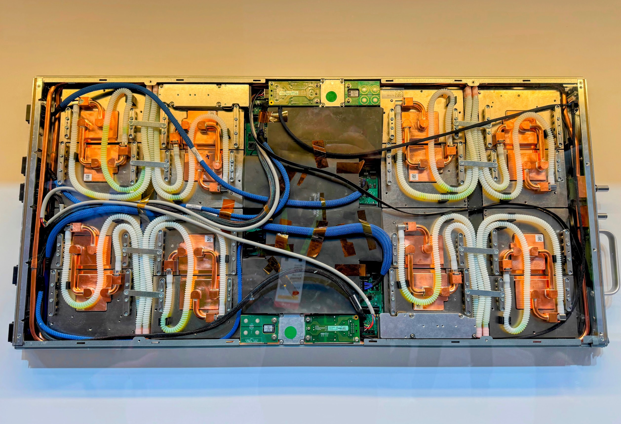
Intel has developed a 4 Tbps bidirectional totally built-in OCI chiplet based mostly on Intel’s in-house Silicon Photonics know-how, to deal with the AI infrastructure’s super want for bandwidth and to allow future scalability. This OCI chiplet or tile accommodates a single Silicon Photonics Built-in Circuit (PIC) with built-in lasers, {an electrical} IC with RF By-Silicon-Vias (TSV), and a path to include a removable/re-usable optical connector.

Intel 4 Tbps Optical Compute Interconnect (OCI) Chiplet
The OCI chiplet could be co-packaged with next-generation CPU, GPU, IPU, and different System-On-a-Chip (SOC) purposes with excessive bandwidth demand. This primary implementation paves the way in which towards offering multi-Terabit optical connectivity with a >4x enchancment in shoreline density over PCIe Gen6, an vitality effectivity of
We plan to display our first-generation OCI chiplet co-packaged with an idea Intel CPU operating dwell error-free visitors over fiber, at OFC 2024 in San Diego on March 26-28 (Intel sales space #1501). This primary OCI implementation is a 4 Tbps bidirectional chiplet appropriate with PCIe Gen5, supporting 64 lanes of 32 Gbps knowledge in every path over 10’s of meters, realized as eight fiber pairs every carrying eight DWDM wavelengths. Wanting past this primary implementation, the platform has line of sight to 32 Tbps chiplets.


Idea Intel CPU with co-packaged OCI

OCI Transmitter: Optical spectrum of 8 wavelengths on one commonplace single-mode fiber
The only PIC within the present die-stack can assist as much as 8 Tbps bidirectional purposes and it accommodates a whole optical sub-system, enabled by Intel’s distinctive functionality of integrating DWDM laser arrays and optical amplifiers on the PIC, offering orders of magnitude of upper reliability than standard InP lasers. These built-in Silicon Photonics chips are manufactured at considered one of our high-volume fabs within the US, which has already shipped greater than 8 million PICs with over 32 million on-chip lasers embedded in pluggable optical transceivers for knowledge middle networking, with industry-leading reliability. In addition to efficiency benefits and confirmed reliability, the on-chip laser know-how allows true wafer-scale manufacturing, burn-in, and testing, which interprets into excessive subsystem-level simplicity and reliability (e.g., there are not any fibers connecting the ELS and PIC) and manufacturing efficiencies.
An extra differentiating benefit is that OCI makes use of commonplace, broadly deployed single-mode fiber (SMF-28), with out requiring Polarization Sustaining Fiber (PMF) like different technical approaches available in the market. PMF has been not often deployed, as system vibration and fiber wiggle can negatively have an effect on its efficiency and related hyperlink price range.
A number of teams inside Intel are contributing to the event and implementation of OCI as a key enabling optical I/O know-how. It highlights how Intel can supply a whole next-generation compute resolution with our main silicon, optical, packaging, and platform integration capabilities.
Intel’s field-proven Silicon Photonics know-how and platform can present the best efficiency and most dependable optical connectivity options to make ubiquitous AI potential.